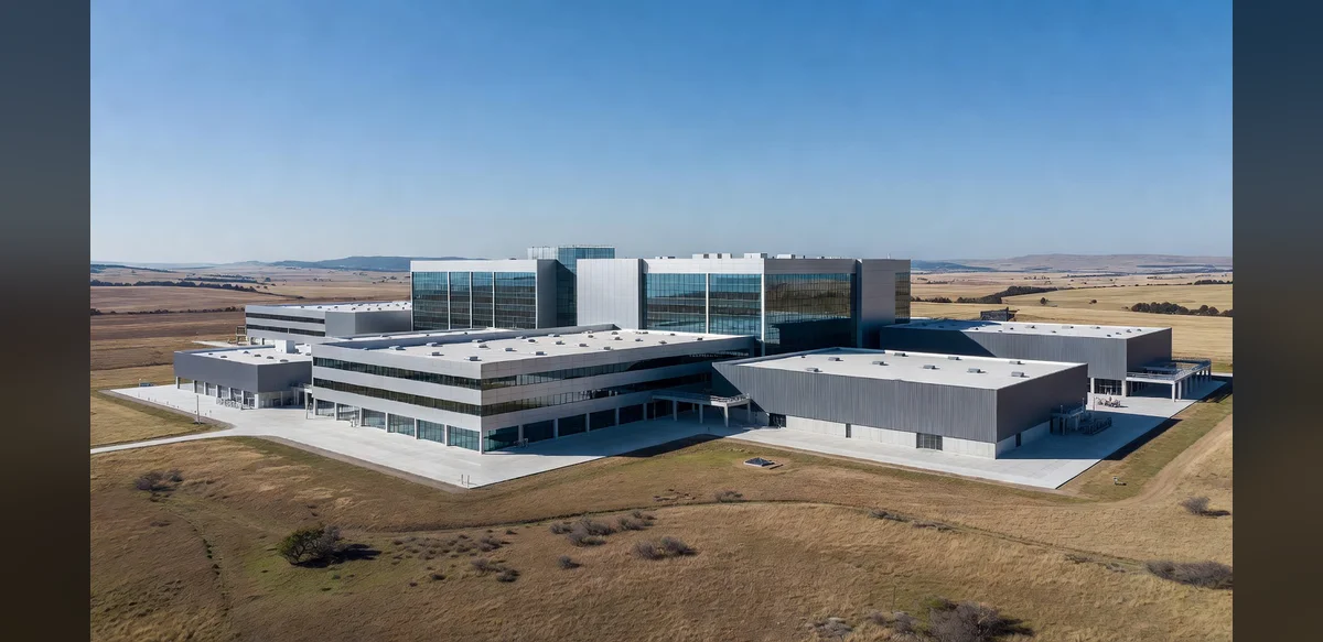
A leading memory chip manufacturer has announced plans for a substantial new facility focused on advanced packaging processes. The project, valued at approximately four billion dollars, will be located in Indiana and is intended to establish domestic capabilities for high bandwidth memory production. This development comes amid ongoing efforts to address vulnerabilities in global semiconductor supply networks.
The initiative targets a key area of semiconductor manufacturing known as advanced packaging. This stage involves assembling and interconnecting chips in ways that improve performance and efficiency. By bringing such capabilities to the United States, the project seeks to reduce reliance on overseas facilities for critical components used in data centers, artificial intelligence systems, and high performance computing applications.
Industry observers note that high bandwidth memory plays an essential role in modern electronics. Demand for these specialized memory chips has grown rapidly due to their ability to handle large data volumes at high speeds. Establishing production capacity within the country could help mitigate risks associated with international shipping delays, geopolitical tensions, and concentrated manufacturing in specific regions.
The chosen location in Indiana offers several advantages for large scale industrial projects. The state provides access to necessary infrastructure, a skilled workforce, and supportive local policies for technology investments. Construction of the facility is expected to create numerous jobs during both the building phase and subsequent operations.
Supply chain resilience has become a priority for governments and companies worldwide. Recent disruptions have highlighted how concentrated production of advanced components can lead to shortages affecting multiple sectors. The new packaging plant represents one step toward diversifying sources and building redundancy into the system.
While the project focuses on packaging rather than front end wafer fabrication, it addresses an important gap. Advanced packaging techniques are increasingly vital for achieving the performance levels required by next generation processors. Integrating these processes domestically supports broader goals of technological self sufficiency.
The investment reflects wider trends in the semiconductor industry. Companies are evaluating their global footprints and considering additional sites to balance cost, capability, and security considerations. Partnerships between manufacturers and regional authorities often facilitate such expansions through incentives and regulatory support.
Stakeholders emphasize that successful execution will depend on timely construction, workforce development, and integration with existing supply networks. The facility is projected to contribute to national objectives around semiconductor leadership and economic competitiveness.
Overall, the announcement underscores the strategic importance of memory technologies and packaging expertise. As computing demands continue to rise, investments of this nature aim to ensure stable access to essential components while fostering innovation in related fields.