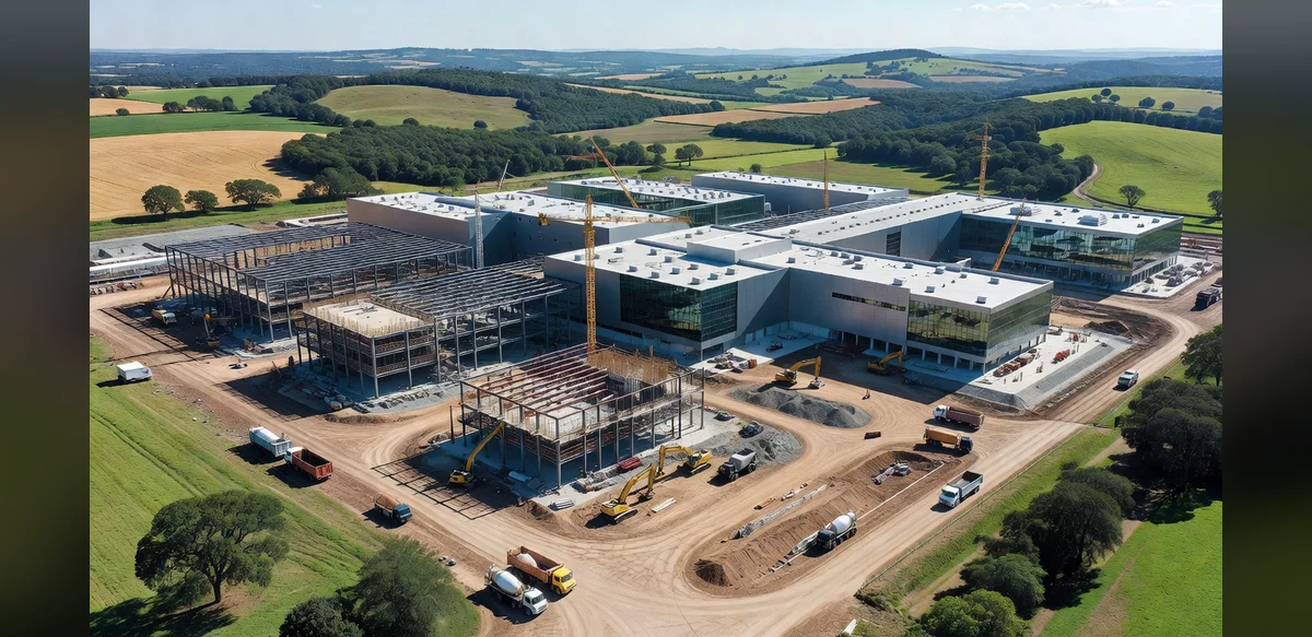
Sony and TSMC have confirmed plans to allocate 6.3 billion dollars toward the development of an advanced image sensor production site located in Kumamoto. The project represents a significant capital commitment aimed at expanding manufacturing capabilities in this specialized sector.
The announcement highlights the strategic focus on enhancing production infrastructure for high-performance image sensors. These components play a central role in various electronic devices and applications. The facility is expected to incorporate state-of-the-art processes to meet evolving technical requirements.
Local authorities in Kumamoto have been informed of the investment, which is anticipated to contribute to regional economic activity through job creation and supply chain development. The scale of the funding underscores the importance placed on advancing semiconductor-related manufacturing.
Industry observers note that such investments reflect ongoing efforts to strengthen global production networks for critical electronic parts. The collaboration between the two companies combines expertise in sensor technology and fabrication techniques.
Construction timelines and operational details remain subject to further planning and regulatory approvals. The project is positioned to support long-term growth in the image sensor market by increasing output capacity.
Stakeholders emphasize the neutral commercial nature of the venture, with no immediate changes expected to existing market dynamics. The investment aligns with broader trends in technology infrastructure expansion.
Further updates on the Kumamoto site are likely to be released as milestones are reached. This development marks one of the larger recent commitments in the field of advanced sensor production.
The 6.3 billion dollar figure encompasses land acquisition, building construction, equipment installation, and initial operational setup. Project managers will oversee phased implementation to ensure efficient resource allocation.
Regional supply chains may benefit from the influx of activity associated with the new plant. Suppliers of raw materials and support services could see increased demand over time.
Overall, the initiative demonstrates continued interest in specialized manufacturing locations outside traditional hubs. Kumamoto offers suitable geographic and logistical advantages for the endeavor.
Monitoring of progress will continue through official channels. The companies involved have expressed commitment to completing the facility according to established standards.
This investment stands as a clear example of corporate strategy in the electronics manufacturing domain. It focuses exclusively on expanding physical production assets for image sensors.
Additional context includes the general importance of image sensors in consumer and industrial products. The new site aims to address future demand through enhanced technological capabilities.
No alterations to current product lines or market strategies have been indicated beyond the scope of this specific project. The emphasis remains on the physical development in Kumamoto.
The total investment amount has been verified through company statements. It positions the facility among notable projects in the semiconductor supply chain.
Economic contributions are expected to accrue gradually as construction advances and operations commence. Local employment opportunities may arise during both phases.
In summary, the Sony and TSMC plan centers on a substantial financial outlay for an image sensor plant. The location in Kumamoto provides the foundation for this expansion effort.
Ongoing reporting will track any subsequent developments related to the initiative. The core facts of the announcement remain centered on the stated investment and purpose.